忘忧草社区在线观看视频,春暖花开性8论坛新版入口,角头1电影在线看免费,福利天堂社区论坛入口,丁香五月天图片区小说区,欧美2025hd变态,午夜免费1000集757,亚欧综合免费视频在线观看完整版

Shenzhen Grande Electronic Linkedin Page
Shenzhen Grande Electronic Co., Ltd logo
E-mail us for a Quote:
sales88@greattong.com
Call us now:
+86-755-83261869

Technical Article


What does a “footprint” mean in PCB design?

Time:2019-06-03 14:38:02 Click:

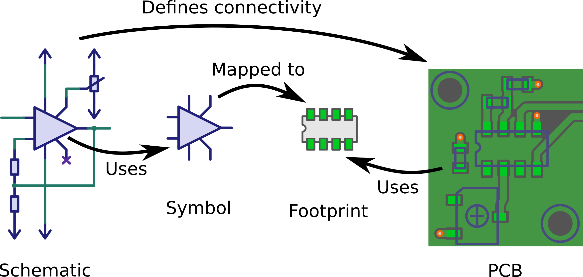
A footprint is called a "land pattern", which is mainly used during PCB layout so that an electronic component gets soldered onto the PCB conveniently. Furthermore, footprint still consists of several layers information, including the copper lands, silkscreen (the text and shapes you see when looking at a PCB), solder mask, solder paste, courtyard, etc.


Apart from that, when it comes to the characteristics of a footprint, I have to say, it is various and based on the mechanical dimensions and tolerances of component, that's to say, the corresponding standard is used to create the footprint and design requirements.


In a nutshell, with the help of complete footprint, PCB designers tend to understand relevant components and do PCB layout easily.


Previous:Are IC package dimensions standard?

Next:How can I understand each component of a circuit board?


Request an Official Quote

Questions

E-MAIL

File Upload

Upload a list of files

    Please upload your Gerber files and BOM. You can upload an unlimited number of files as long as the total size of all files does not exceed 20 MB. To ensure you receive your official quote in less than 24 hours, please include the quantity of circuit boards for which you would like a quote.

    If you require that we sign a Non-Disclosure Agreement (NDA), please send it to us prior to sending your files and we will be happy to accommodate.

     
    Home About Us Services Quality Pb-Free News Contact Us


    Copyright ® 2017,Shenzhen Grande Electronic Co., Ltd. All Rights Reserved. English 中文站 Sitemap

    忘忧草社区在线观看视频,春暖花开性8论坛新版入口,角头1电影在线看免费,福利天堂社区论坛入口,丁香五月天图片区小说区,欧美2025hd变态,午夜免费1000集757,亚欧综合免费视频在线观看完整版